Quick Navigation
- Introduction to Differential Signaling
- Why Differential Signaling Matters
- Understanding Differential Pair Fundamentals
- Common Differential Signal Standards
- USB 2.0 Differential Pair Routing
- Critical Placement Considerations
- Differential Pair Routing Rules
- Differential Pair Routing Guidelines (Stackup & Plane Selection)
- Routing Differential Pairs: Step-by-Step
- Differential Routing Best Practices
- Advanced Routing Techniques
- Common Design Challenges and Solutions
- Design Verification and Testing
- Modern Automation in Differential Design
- Conclusion and Best Practices Summary
- Frequently Asked Questions
Introduction to Differential Signaling
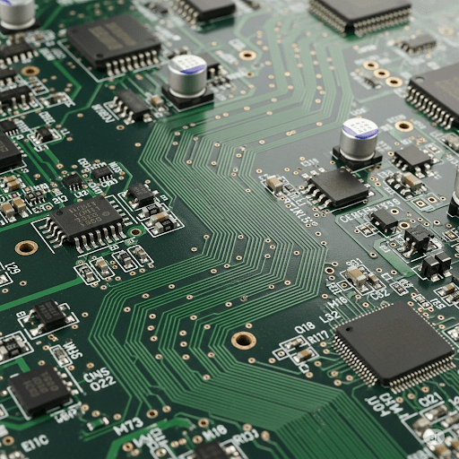
In today's high-speed digital world, differential signaling has become essential for reliable data transmission in PCB designs. From USB and Ethernet to high-speed memory interfaces and display connections, routing differential pairs correctly is one of the more demanding tasks in PCB layout - and one where errors tend to surface late. Understanding how to properly place and route these critical signals can make the difference between a working design and one plagued by signal integrity issues.
This comprehensive guide covers the fundamental principles, practical considerations, and modern approaches to differential pair design - including placement strategy, routing rules, and verification steps.
Why Differential Signaling Matters
Differential signaling offers significant advantages over single-ended signals:
- Superior noise immunity: Common-mode noise affects both traces equally and cancels out
- Reduced EMI emissions: Equal and opposite currents minimize electromagnetic radiation
- Better signal integrity: Controlled impedance and balanced transmission
- Higher data rates: Enables faster switching speeds with cleaner signals
- Lower power consumption: Smaller voltage swings reduce power requirements
Understanding Differential Pair Fundamentals
What Are Differential Pairs?
A differential pair consists of two complementary signals (often labeled P and N, or + and -) that carry the same information but with opposite polarity. The receiver detects the voltage difference between these two signals rather than their absolute voltage levels. This approach provides inherent noise rejection because any noise that affects both traces equally (common-mode noise) is ignored by the differential receiver.
Key Electrical Parameters
| Parameter | Typical Values | Description |
|---|---|---|
| Differential Impedance (Zdiff) | 90Ω, 100Ω, 120Ω | Impedance between the two traces in the pair |
| Common-Mode Impedance (Zc) | 25-60Ω | Impedance of each trace to ground |
| Coupling Coefficient (k) | 0.1-0.3 | Degree of electromagnetic coupling between traces |
| Skew Tolerance | ±10% of rise time | Maximum acceptable delay mismatch |
Key Relationships:
Where Z0 is the single-ended impedance and k is the coupling coefficient
Common Differential Signal Standards
Different protocols require specific impedance values and design considerations. Here's a comprehensive overview of common differential signal standards:
| Protocol | Differential Impedance | Tolerance | Key Considerations |
|---|---|---|---|
| USB 2.0 | 90Ω | ±15% | Skew ≤150 ps (≈2.5 mm), short stubs, maximum 3m cable length |
| USB 3.0/3.1 | 90Ω | ±7% | Tight skew requirements ≤25 ps, strict impedance control, separate from USB 2.0 pairs |
| Ethernet 10/100 | 100Ω | ±5% | Transformer isolation required, moderate skew tolerance |
| Gigabit Ethernet | 100Ω | ±5% | Strict skew requirements ≤100 ps, all 4 pairs must be matched, ground plane continuity critical |
| HDMI | 100Ω | ±15% | Multiple differential pairs (TMDS), skew ≤40 ps within pair, ESD protection needed |
| PCIe Gen1/2 | 85Ω | ±7% | Skew ≤20 ps, AC coupling required, strict layer stackup requirements |
| PCIe Gen3/4 | 85Ω | ±5% | Very tight skew ≤10 ps, loss budget critical, requires simulation validation |
| SATA | 100Ω | ±15% | AC coupling caps required, ground plane under traces, via count minimization |
| DDR4 | 100Ω (clock, DQS) | ±10% | Topology-dependent routing, on-die termination, fly-by architecture for address/command |
| DDR5 | 80-100Ω (varies) | ±8% | Higher speeds require tighter control, decision feedback equalization impacts design |
| LVDS | 100Ω | ±10% | Low voltage swing (±350mV), excellent EMI performance, common in displays and cameras |
| CAN Bus | 120Ω | ±10% | Termination resistors required at both ends, robust to EMI, automotive applications |
| DisplayPort | 100Ω | ±10% | Multiple lanes, auxiliary channel separate, pre-emphasis and equalization support |
| MIPI D-PHY | 100Ω | ±15% | Mobile display/camera interface, LP (low power) and HS (high speed) modes |
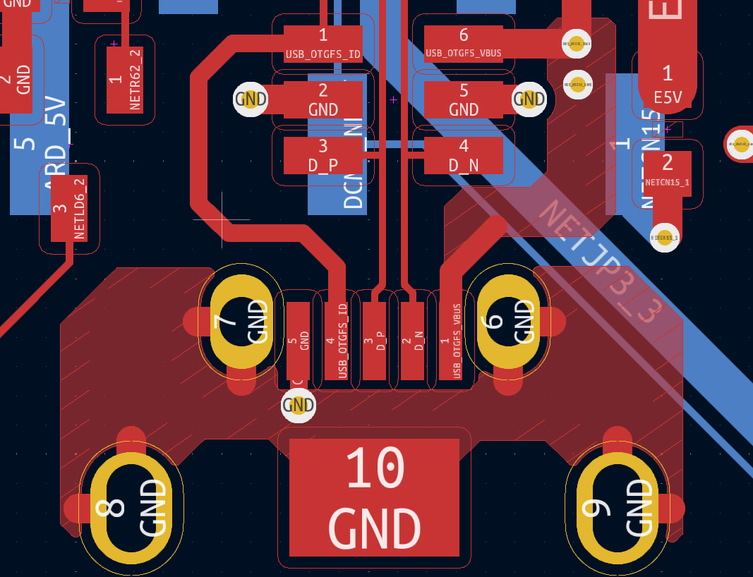
USB 2.0 Differential Pair Routing
USB 2.0 High-Speed is one of the most common differential interfaces on PCBs, and its routing requirements are well-defined. The interface uses a 90Ω differential impedance with a ±15% tolerance, which is more forgiving than USB 3.0 but still requires deliberate stackup planning.
Key USB 2.0 Differential Pair Requirements
| Parameter | Requirement | Notes |
|---|---|---|
| Differential Impedance | 90Ω ±15% | Derive width/gap from your stackup using a field solver |
| Intra-pair skew | ≤150 ps (≈25 mm on FR-4) | Many designers target ≤5 mm for margin |
| Differential voltage swing | ~400 mV peak-to-peak at receiver | Current-driven; maintain impedance to preserve eye opening |
| Uncoupled stub length | ≤2–3 mm | Applies to pad breakouts and test point spurs |
| Inter-pair matching | Not required | Only intra-pair (D+ to D−) skew matters for USB 2.0 |
USB 2.0 Routing Checklist
- Route D+ and D− together: Keep the pair coupled from connector to IC; avoid splitting them across layers unless absolutely necessary
- Avoid stubs: Keep unused branch lengths under 2–3 mm; stubs create reflections that degrade the eye
- Single reference plane: Route over a continuous ground plane; do not cross plane splits
- Minimize vias: Each via transition introduces discontinuity; co-locate P and N vias and add a stitching via within 1–2 mm
- ESD protection placement: Place TVS diodes close to the connector, route through them before reaching the IC
- Separate from USB 3.0 pairs: If USB 3.0 SuperSpeed pairs are present on the same connector, route them on a separate layer with adequate spacing
⚠️ Common USB 2.0 Routing Mistake
Routing D+ and D− as individual signals rather than a constrained differential pair. Always assign them to a net class with the 90Ω differential impedance rule before routing — this ensures your tool enforces consistent width, gap, and coupling throughout the route.
Critical Placement Considerations
Component Proximity and Grouping
Proper placement is the foundation of successful differential routing. The physical arrangement of components directly impacts signal integrity, routing complexity, and overall design success.
Strategic Placement Guidelines
- Minimize trace lengths: Place differential sources and loads as close as possible
- Group related components: Keep all components for a differential interface together
- Consider pin escape: Ensure differential pins can exit components cleanly
- Plan layer transitions: Minimize via count in differential paths
- Isolate sensitive circuits: Keep high-speed differential away from sensitive analog
- Account for termination: Reserve space for termination resistors and AC coupling
Connector and Interface Placement
Connector placement significantly impacts differential routing success. Modern automated placement algorithms consider multiple factors simultaneously:
💡 Pro Tip: Automated Placement Intelligence
Advanced placement algorithms analyze pin assignments, trace length requirements, and layer escape strategies to optimize connector positions. This multi-constraint optimization often yields better results than manual intuition alone, especially for complex boards with multiple differential interfaces.
✅ DO
- Position connectors for short, direct paths
- Align differential pins for parallel routing
- Consider mechanical constraints early
- Plan for proper ground references
- Group related differential interfaces
❌ DON'T
- Place connectors without considering routing
- Ignore pin assignment optimization
- Create unnecessary layer transitions
- Split differential interfaces across board
- Overlook return path requirements
Differential Pair Routing Rules
Keep the two traces tightly coupled and parallel, reference the same continuous return plane, and keep any uncoupled stubs as short as possible. Co-locate vias in pairs, minimize layer transitions, and match lengths within your skew budget computed from the stackup.
Essential Routing Rules
- Net Naming: Define pairs with a clear suffix (_P/_N) and put them in a net class
- Via Management: Keep same number of vias on P and N; place stitching vias near any plane transition
- Route Geometry: Prefer straight routes; if you must meander, meander both partners
- Uncoupled Length: Enforce maximum uncoupled length (breakouts, pads, test points)
- Impedance Control: Use stackup-based width/gap (not "rules of thumb") for target Zdiff
Differential Pair Routing Guidelines
Choose width/gap from your stackup to hit the required Zdiff (e.g., 90Ω USB HS, 100Ω Ethernet/PCIe/LVDS). Route over a single reference plane per segment; if you must cross a split, provide a stitching path for the return current within ~1–2 mm.
Critical Guidelines
- Reference Planes: Avoid reference plane gaps; if unavoidable, bridge with stitching capacitors/vias as appropriate
- Pair-to-Pair Spacing: Keep pair-to-pair spacing ≥ 3× the intra-pair gap to reduce crosstalk
- Layer Selection: Prefer microstrip for short, simple runs; prefer stripline for dense, noisy boards
- Connector Breakouts: Treat connector breakouts like controlled impedance features; follow vendor land patterns
Routing Differential Pairs: Step-by-Step
Routing differential pairs follows a consistent process regardless of the protocol. Whether you are working with USB, Ethernet, PCIe, or LVDS, the steps below apply. Skipping or reordering them is the most common cause of rework.
Step 1: Define the Net Class Before You Route
Set up your differential pair net class in your EDA tool before placing a single trace. This means naming the nets consistently (e.g., USB_DP / USB_DM, or ETH_TX+ / ETH_TX−), assigning them to a differential pair rule, and setting the target impedance, width, gap, and maximum uncoupled length. Routing without these rules in place means your tool cannot enforce symmetry or flag violations as you go.
Step 2: Determine Width and Gap from Your Stackup
Do not use generic trace width tables. Get the controlled impedance width and gap from your PCB fabricator's stackup, or calculate them using a field solver with the actual dielectric properties of your board material. For a typical 4-layer FR-4 board targeting 90Ω differential (USB), this is commonly around 0.15 mm width and 0.18 mm gap on an outer microstrip layer — but your stackup will differ. Lock these values in your design rules before routing.
Typical Starting Points (Always Verify with Your Fab)
| Protocol | Target Zdiff | Typical Layer Type | Notes |
|---|---|---|---|
| USB 2.0 | 90Ω | Outer microstrip | Verify with fab stackup solver |
| Ethernet / PCIe / LVDS | 100Ω | Outer or inner stripline | Stripline preferred for noisy boards |
| PCIe Gen3/4 | 85Ω | Inner stripline | Requires simulation validation |
Step 3: Plan the Route Before Drawing It
Trace the path mentally from source to load. Identify where layer transitions will occur, whether a reference plane split exists anywhere along the path, and where space constraints may force the pair apart. Resolving these issues during planning — rather than mid-route — avoids the common problem of routing yourself into a corner and having to undo significant work.
- Identify layer transitions early: Each via transition needs a stitching via nearby; plan for the space
- Check for plane splits: If the path crosses a split, plan a stitching capacitor or reroute to avoid it
- Note any tight spaces: BGA breakouts and connector pin fields often require the pair to briefly uncoupled — plan how to minimize that length
Step 4: Route the Pair Coupled and Parallel
Start routing from the source (typically an IC pin or connector) and keep both traces locked together as a differential pair throughout. Do not route one trace and then match the other — route them simultaneously using your tool's differential pair router. Maintain the defined gap consistently; avoid widening or narrowing it mid-route. Keep the pair on the same layer wherever possible.
✅ DO
- Use your tool's differential pair routing mode
- Maintain consistent gap throughout the route
- Keep both traces on the same layer
- Route over a single continuous reference plane
- Keep the route as direct as practical
❌ DON'T
- Route P and N as individual single-ended traces
- Change width or gap mid-route
- Split the pair across different layers without co-located vias
- Cross a reference plane split without stitching
- Add unnecessary length to one trace only
Step 5: Handle Connector and IC Breakouts Carefully
The breakout region — where the pair exits a BGA, connector, or IC — is where the traces are most likely to be briefly uncoupled. Keep this uncoupled length under 2–3 mm. Use the shortest path out of the pin field and re-couple the pair as soon as clearance allows. Avoid routing over a via or plane cutout in the breakout zone.
Step 6: Manage Layer Transitions
When the pair must change layers, always transition both traces together at the same location. Place P and N vias as a matched pair with identical antipads. Add a ground stitching via within 1–2 mm of the transition to maintain the return path. Verify in your length report that P and N have identical via counts — a single extra via on one trace introduces asymmetry that cannot be corrected with length matching alone.
Step 7: Match Lengths Last
Length matching is the final step, not a starting point. First match the route topology — same number of vias, same layer sequence, same general path. Then use your tool's length tuning to add meanders to the shorter trace to bring it within your skew budget. Use gentle curves rather than sharp U-turns, keep meanders away from the coupled segment of another differential pair, and minimize the total meander length added.
💡 Length Matching Order of Priority
- Match via count (P and N must be equal)
- Match layer sequence (same transitions in the same order)
- Match path topology (similar routing path)
- Add serpentine meanders only for the remaining delta
Step 8: Run DRC and Review
After routing, run a differential pair DRC to check impedance rule compliance, uncoupled length violations, via asymmetry, and length mismatch against your skew budget. Review the length report for every pair — do not rely on visual inspection alone. For high-speed interfaces like USB 3.0, PCIe Gen3/4, or DDR, consider running a pre-layout or post-layout simulation to verify eye opening before sending to fabrication.
Differential Routing Best Practices
Trace Geometry and Spacing
The physical geometry of differential traces directly affects their electrical performance. Proper spacing, width, and layer selection are crucial for maintaining target impedance and ensuring reliable signal transmission.
Critical Routing Parameters
Spacing Calculations:
Center-to-center spacing = W + s
Where W = trace width
Length Matching Requirements
Maintaining proper length matching between differential pair traces is essential for signal integrity. Different protocols have varying tolerance requirements:
| Protocol | Skew Tolerance | Matching Requirement |
|---|---|---|
| USB 2.0 | ±150 ps | ±2.5mm at PCB level |
| USB 3.0 | ±25 ps | ±0.1mm (very tight) |
| Gigabit Ethernet | ±100 ps | ±1.5mm at PCB level |
| PCIe Gen1/2 | ±20 ps | ±0.3mm within pair |
| HDMI | ±40 ps | ±0.6mm within pair |
Layer Transitions and Via Management
Differential signals often need to change layers, requiring careful via placement and return path management.
Key considerations for via transitions include proper return path management, impedance control, and minimizing discontinuities. Advanced routing algorithms can automatically handle these requirements while maintaining signal integrity.
⚠️ Via Transition Considerations
- Always transition differential pairs together (same location)
- Provide return path stitching vias nearby
- Account for via impedance discontinuity
- Minimize the number of layer transitions
- Consider stub length for non-through vias
Advanced Routing Techniques
Curved vs. Angular Routing
The choice between curved and angular routing affects both signal integrity and manufacturing considerations. Modern routing engines typically favor curved approaches for their superior electrical performance.
Routing Style Comparison
Curved Routing Advantages
- Smoother impedance transitions
- Reduced EMI emissions
- Better high-frequency performance
- More aesthetically pleasing
- Easier length matching
Angular Routing Considerations
- Impedance discontinuities at corners
- Potential EMI hotspots
- More complex length matching
- Traditional but less optimal
- Still acceptable for lower speeds
Serpentine Routing for Length Matching
When differential traces need length matching, serpentine (meandering) sections are often required. The key is using gradual curves rather than sharp corners, maintaining consistent spacing throughout serpentines, and placing them away from sensitive circuits.
💡 Serpentine Best Practices
- Use gradual curves rather than sharp corners
- Maintain consistent spacing throughout serpentines
- Place serpentines away from sensitive circuits
- Consider the impact on impedance and crosstalk
- Minimize the serpentine section length
Preferred Differential Pair Signal Gap
The "right" gap is whatever your stackup solver returns for the target impedance and selected trace width. As a quick start, many 4-layer FR-4 microstrips hit 90Ω with ~0.14–0.18 mm width and ~0.16–0.22 mm gap, but always verify with your fab's stackup.
Gap Selection Process
- Use Field Solver: Use your fab's field solver
- Lock Geometry: Lock gap and width per layer; avoid changing geometry mid-route
- Maintain Spacing: Keep pair-to-others spacing ≥ 3× gap
How to Flip Vias in Differential Pairs
Place P and N vias as a matched pair with identical antipads and keep them as close as DRC allows; route short necks into the pair to avoid length asymmetry. When changing reference planes, add a stitching via within ~1–2 mm to provide a return path.
Via Placement Best Practices
- Routing Strategy: Route into the center of the via pair; avoid doglegs on only one partner
- Via Consistency: Same via count and drill for P and N; avoid via stubs (backdrill if needed)
- Length Verification: Verify with length report: P and N through-via lengths must be matched
Test Point Placement in Differential Pairs
Avoid in-line test pads on high-speed pairs; if you must, place symmetrical pads on both P and N and keep them very small or use probe pads on a short coupled spur. Favor connector-side fixtures and AC-coupled test methods over intrusive pads.
Test Point Guidelines
- Spur Length: If you must tee off, keep the spur ≤ 1–2 mm and matched on both lines
- Integrated Probing: Consider footprint-integrated probing (e.g., header pads at connector breakouts)
Routing a 1 GHz Differential Output to Multiple Connectors
⚠️ Critical Design Constraint
Splitting a high-frequency differential pair creates stubs and impedance discontinuities. It is not recommended. If you need to do it then document expected return loss/eye degradation; validate on the SI tools of your choice.
Differential Via Transition
Treat the via pair as part of the transmission line; keep antipads/clearances consistent and add stitching vias to maintain the return path. Avoid long plated stubs (use backdrilling or blind/buried vias if available).
Via Transition Guidelines
- Via Spacing: Co-locate the pair; center-to-center distance ≈ intra-pair gap is a good start
- Plane Transitions: Keep plane transitions minimal and symmetric
Common Design Challenges and Solutions
Routing in Constrained Spaces
Modern PCB designs often face space constraints that make differential routing challenging. Proven strategies include via-in-pad techniques, blind/buried vias, layer stack optimization, and intelligent component orientation.
Space-Constrained Solutions
- Via-in-pad techniques: For BGAs and high-density designs
- Blind/buried vias: Reduce via count and improve routing density
- Layer stack optimization: Choose appropriate layer pairs for routing
- Component orientation: Rotate components for better pin escape
- Micro-via technology: Enable finer routing pitch
Managing Multiple Differential Pairs
Designs with numerous differential interfaces require systematic approaches to avoid conflicts and maintain signal integrity. This involves prioritizing critical signals, grouping by speed requirements, and maintaining proper isolation between different pairs.
Multi-Pair Design Guidelines
- Prioritize critical signals: Route timing-sensitive pairs first
- Group by speed: Separate high-speed and low-speed differential signals
- Maintain isolation: Provide adequate spacing between different pairs
- Plan layer assignments: Distribute pairs across multiple layers
- Consider crosstalk: Account for near-end and far-end crosstalk
- Validate timing: Ensure all pairs meet their timing requirements
Design Verification and Testing
Simulation and Analysis
Proper verification ensures your differential design will work reliably in the real world:
Essential Verification Steps
- Impedance analysis: Verify differential and common-mode impedance
- Crosstalk simulation: Check for excessive coupling between pairs
- Eye diagram analysis: Assess signal quality at the receiver
- Return loss analysis: Identify impedance discontinuities
- Power integrity: Ensure clean power delivery to differential circuits
- EMI compliance: Validate emissions and immunity requirements
Physical Testing Considerations
Design your PCB with testing in mind from the beginning:
- Test point placement: Provide access for differential probing
- TDR test structures: Include impedance verification features
- Loop-back paths: Enable signal integrity testing
- Debug headers: Provide access to critical differential signals
- Ground probe points: Ensure proper measurement references
Modern Automation in Differential Design
What Automation Can and Cannot Do
Automated placement and routing tools can handle well-defined, rule-driven tasks such as enforcing consistent trace width and gap, co-locating via pairs, and flagging uncoupled length violations. They work best when design rules are fully specified before routing begins. They are not a replacement for understanding the underlying electrical requirements - a poorly configured rule set will produce a plausible-looking but incorrect result.
Placement algorithms can cluster related components and consider pin escape constraints, which helps reduce routing complexity for differential interfaces. Manual review of placement - particularly for sensitive components like crystals and RF circuits - remains necessary before routing begins.
Modern routing engines can enforce impedance-driven width and gap rules, co-locate via transitions, and help with length matching. The quality of the output depends directly on how well the net classes, stackup, and constraints are configured going in.
- Consistency: Differential pair rules are applied uniformly across the design rather than relying on manual judgment for each pair
- Reduced iteration: Rule-driven routing can surface violations earlier in the process, reducing late-stage rework
- Starting point: Automation can produce an initial routed result that engineers then review and refine - it is not a substitute for engineering judgment
- Embedded guidelines: Design rules can encode known-good practices for common protocols, reducing the chance of overlooking a requirement
- Iteration support: Re-running placement or routing after constraint changes is faster than redoing it manually from scratch
Conclusion and Best Practices Summary
Successful differential signal design requires careful attention to both placement and routing decisions. The key principles remain consistent across different technologies and protocols:
🎯 Key Takeaways
- Start with placement: Good placement makes routing possible; poor placement makes it impossible
- Understand your requirements: Know the impedance, timing, and spacing requirements for your specific protocols
- Plan for manufacturing: Consider fabrication capabilities and assembly constraints
- Verify early and often: Use simulation to catch problems before fabrication
- Consider automation: Modern tools can handle much of the complexity while maintaining design quality
- Keep learning: High-speed design techniques continue to evolve with technology
Looking Forward
As data rates continue to increase and PCB designs become more complex, the challenges of differential signaling will only grow. Advances in tooling and simulation are making it easier to verify designs before fabrication, but the fundamentals of impedance control, return path management, and length matching remain as important as ever.
A solid grasp of the underlying principles - combined with well-configured design rules and a methodical routing process - is what leads to reliable, manufacturable differential pair designs.
Frequently Asked Questions
Want to Know More About How We Use AI with PCB Design?
Check out our comprehensive blog covering AI-assisted PCB design verification across Altium, Cadence, KiCad and other tool series.
Blogs